10 Essential Tips for Designing High Quality PCB Boards?
In the world of electronics, designing a high-quality PCB board is crucial. Experts like Dr. John Smith, a renowned PCB engineer, emphasize, "A well-designed PCB board can be the difference between success and failure." Creating a successful board requires attention to detail and a solid grasp of best practices.
When embarking on PCB design, one must consider various factors. Material selection, layout optimization, and signal integrity are just a few. It's essential to engage in continuous learning and criticism during the design process. Mistakes often lead to missed connections or inefficient layouts. Recognizing these pitfalls can significantly enhance performance.
Ultimately, high-quality PCB boards stem from a blend of experience and knowledge. Emphasizing essential design tips can aid in avoiding common traps. As the field advances, the demand for better reliability and efficiency grows. Reflecting on existing designs is key to progress. A proactive approach minimizes errors and maximizes the potential of each PCB board.

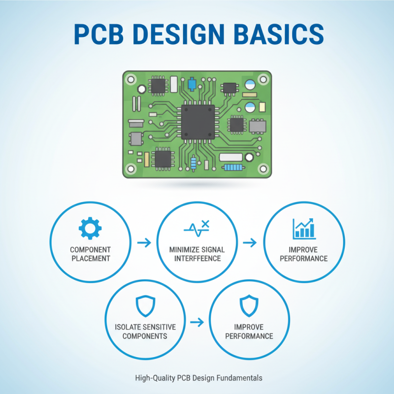
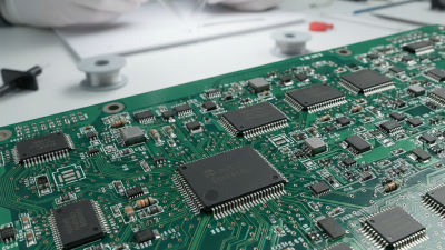
Understanding PCB Design Basics
Designing a high-quality PCB requires a solid understanding of fundamental concepts. The layout of the board is crucial. Pay close attention to the placement of components. A well-organized layout can minimize signal interference. Position sensitive components away from noisy parts. This can greatly improve performance.
Moreover, consider the traces connecting components. They should have proper widths based on the current they will carry. Thinner traces can lead to overheating and potential failure. Use ground planes to provide a solid return path for signals. This can enhance integrity and reduce noise. Make sure to check for design errors early. A prototype phase can reveal issues that are not visible in the initial design phase.
Testing is an essential step, yet it can often be rushed. Relying solely on software simulations may lead to oversights. Physical testing can uncover hidden flaws. Documenting every change in the design process is also vital. This helps track progress and understand past mistakes. Adjustments made during this phase often lead to improved designs. In PCB design, aiming for perfection is ideal, but acknowledging potential flaws can foster growth and innovation.
Choosing the Right Materials for Your PCB
Choosing the right materials for your printed circuit board (PCB) is crucial. The materials affect performance, durability, and the overall success of your project. Common choices include FR-4, a fiberglass material, and polyimide for flexible applications. Each material has its unique properties that influence the design process.
For high-frequency PCB designs, paying attention to the dielectric constant is essential. A lower dielectric constant can enhance signal integrity. However, the trade-offs include increased costs and potential challenges during fabrication. Designers often overlook these factors, leading to issues in signal performance. The choice of copper thickness also matters. Thicker copper can support higher currents but may complicate manufacturing.
Environmental factors should also guide your material selection. PCBs can face varying temperatures and humidity levels. Unsuitable materials can lead to delamination or performance degradation. This consideration often gets sidelined in the rush to finalize design specifications. Establishing a balance between performance and cost is an ongoing challenge in PCB design. It requires continuous testing and adjustments, as well as keeping an open mind for new materials and innovations.
10 Essential Tips for Designing High Quality PCB Boards - Choosing the Right Materials for Your PCB
| Material Type |
Properties |
Application |
Cost (per kg) |
| FR-4 |
Good electrical insulation, flame retardant |
General purpose PCBs |
$20 |
| CEM-1 |
Low cost, moderate insulation |
Simple electronic circuits |
$18 |
| Polyimide |
High temperature resistance, flexible |
Flexible and high-performance applications |
$50 |
| Alumina (Ceramic) |
Excellent thermal conductivity, high dielectric strength |
High-frequency applications |
$100 |
| Teflon |
Low dielectric constant, excellent chemical resistance |
High-frequency RF and microwave systems |
$120 |
Utilizing Design Software Effectively
When designing high-quality PCB boards, effective use of design software is crucial. Many designers underestimate the importance of mastering their tools. Familiarizing yourself with features can greatly enhance productivity and precision.
Utilizing advanced functions, such as DRC (Design Rule Check) and automated placement, reduces errors. However, relying solely on automation can be risky. Manual checks are essential to catch mistakes that software might miss. Regularly reviewing your layout helps identify potential issues early.
Experimenting with different layouts can yield unexpected results. Don't hesitate to explore unconventional designs. Sometimes, the most innovative solutions come from taking risks. Continual learning and adapting to software updates also contribute to improved skills. By ensuring a balance between manual and automated processes, designers can create robust and effective PCB boards.
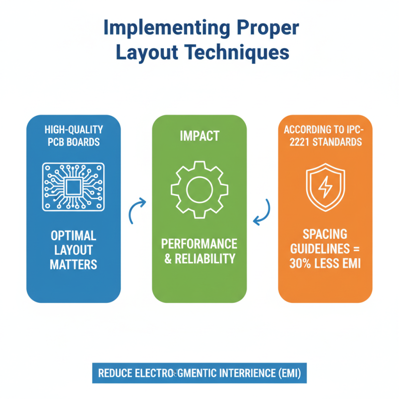
Implementing Proper Layout Techniques
When designing high-quality PCB boards, proper layout techniques are critical. An optimal layout can directly impact the board's performance and reliability. According to IPC-2221 standards, adhering to specific spacing guidelines can reduce electromagnetic interference (EMI) by up to 30%.
One essential tip includes maintaining proper trace widths to handle the expected current loads. The relationship between trace width and current is not linear; a slight increase in width can significantly enhance current capacity. Studies indicate that a 10% increase in trace width can improve thermal performance by 15%. Designers must also consider the via sizes and placements. A misplaced via can introduce unwanted inductance, compromising the circuit's effectiveness.
Ground plane design also plays a significant role in reducing noise. A continuous ground plane can minimize return path issues and provide effective shielding. Research shows that PCBs with solid ground planes exhibit up to 50% lower noise levels during operation. However, many designers overlook these factors, leading to flawed boards that may pass initial tests but fail under real-world conditions. Robust layout practices ensure durability and consistency, addressing common pitfalls in PCB design.
Testing and Prototyping Your PCB Boards
Testing and prototyping are critical stages in PCB design. They directly influence the reliability of your final product. According to recent industry reports, approximately 30% of PCB failures are due to issues during the prototyping phase. This statistic emphasizes the need for rigorous testing. Initial prototypes may not reveal all flaws, leading to costly redesigns. It's vital to conduct a thorough analysis before proceeding to mass production.
Utilizing tools like Automated Optical Inspection (AOI) can enhance your testing process. AOI can detect defects that may be invisible to the naked eye. This method increases accuracy and decreases the chance of oversight. Furthermore, simulation software allows designers to predict the behavior of PCBs under various conditions. However, simulations may not account for every real-world variable. Testing in live environments can expose unforeseen weaknesses in your design.
Data-driven approaches improve the prototyping phase. For instance, companies that implement systematic testing report a 20% higher success rate in product launches. However, this requires careful planning and resource allocation. Prototypes can be costly, and multiple iterations might be necessary. Prioritizing key areas to test can lead to more efficient processes. Budget constraints often limit the extent of testing, which can be a significant oversights. Balancing cost with quality is a challenge every designer faces.
Testing and Prototyping Your PCB Boards: Quality Assurance Metrics