Ultimate Guide to PCB Design and Assembly Best Practices for Beginners
In the ever-evolving landscape of the electronics industry, mastering pcb design and assembly is crucial for both newcomers and seasoned professionals. According to the IPC (Institute of Printed Circuits) report, the global PCB market is projected to reach $70 billion by 2025, highlighting the increasing demand for meticulously designed and assembled printed circuit boards. Additionally, the adoption of advanced technologies such as IoT and wearable devices further emphasizes the importance of understanding best practices in PCB design and assembly. As a fundamental component in all electronic devices, a well-executed PCB not only enhances performance and reliability but also significantly reduces production costs and time-to-market. This ultimate guide serves as a valuable resource for beginners, offering insights into effective strategies and practical tips to navigate the complexities of PCB design and assembly successfully.
Introduction to PCB Design: Understanding the Basics and Importance in Electronics Industry
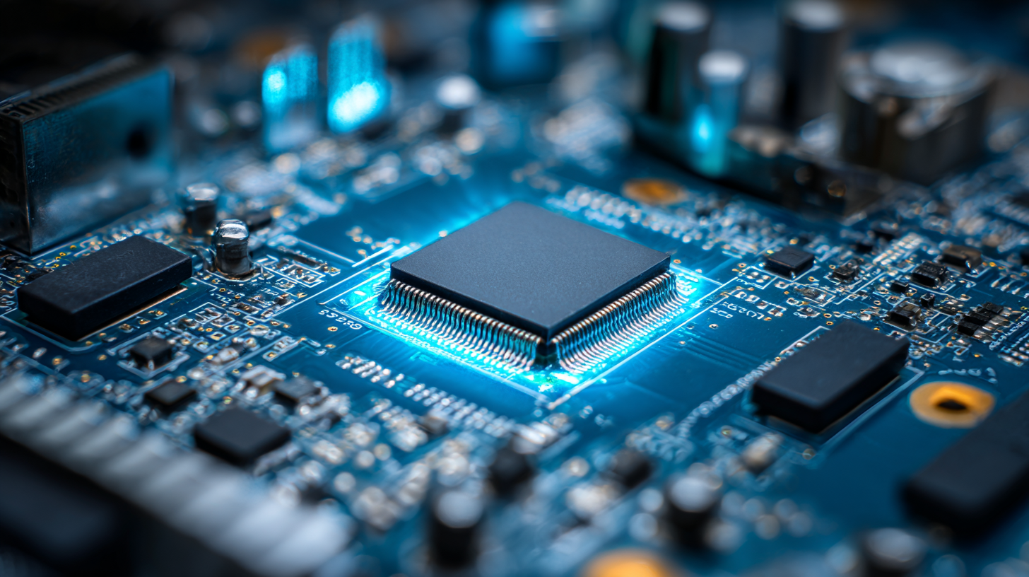
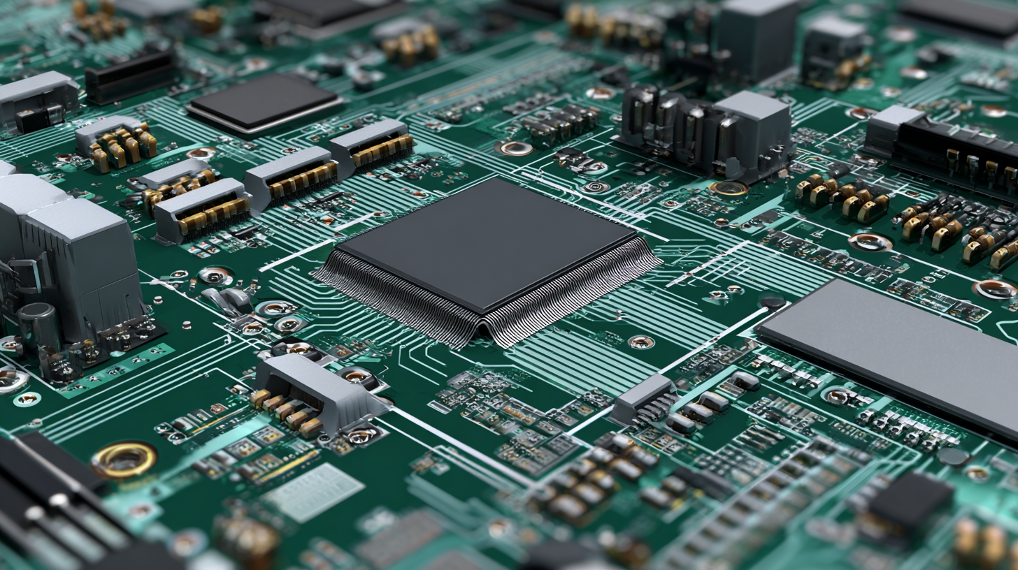
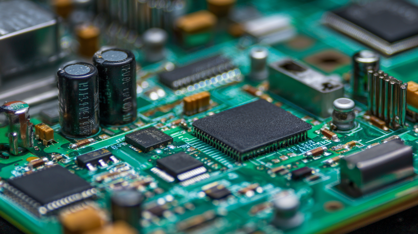 PCB (Printed Circuit Board) design is a fundamental aspect of the electronics industry, serving as the backbone for virtually all electronic devices. Understanding the basics of PCB design is crucial for beginners, as it lays the groundwork for creating functional and efficient electronic systems. At its core, a PCB connects various electronic components, facilitating communication and power distribution. This interconnection is essential not only for the performance of individual devices but also for ensuring the reliability and longevity of the entire electronic system.
The importance of PCB design cannot be overstated, as it directly impacts a product’s overall functionality, cost, and manufacturing scalability. A well-designed PCB can significantly reduce production issues, enhance signal integrity, and minimize electromagnetic interference. For newcomers, grasping the principles of layout, component placement, and routing is vital, as these factors play a pivotal role in the optimization of circuit performance. By mastering these basics, beginners can contribute to innovative designs that meet the growing demands of technology in our daily lives.
Essential Tools and Software for Effective PCB Design and Prototyping
Effective PCB design and prototyping are essential for successful electronic product development. A variety of tools and software have emerged to streamline this process, catering especially to beginners in the field. According to a report by MarketsandMarkets, the global PCB design software market is projected to reach $4.25 billion by 2026, highlighting the growing demand for robust design solutions. Key players like Altium Designer, Eagle, and KiCad offer essential features such as schematic capture, layout design, and simulation capabilities, making them popular choices among new designers.
Additionally, the importance of prototyping cannot be overstated. Rapid prototyping tools, such as 3D printers and CNC machines, provide invaluable support in the development lifecycle. Industry data from Gartner indicates that the adoption of prototyping techniques can reduce time-to-market by up to 20%. Furthermore, PCB manufacturing services like JLCPCB and PCBWay offer affordable options for initial runs, allowing designers to test and iterate designs efficiently. By leveraging these tools and services, beginners can enhance their PCB design skills and effectively transition from concept to tangible products.
Key PCB Layout Techniques: Best Practices to Minimize Signal Integrity Issues
When designing printed circuit boards (PCBs), one of the primary concerns is signal integrity. To achieve optimal signal performance, it is crucial to implement effective layout techniques.
First, maintaining proper trace spacing is essential. Closely spaced traces can lead to crosstalk, which interferes with signal integrity. Designers should ensure adequate separation based on the frequencies involved; generally, a distance of at least three times the trace width is advisable.
Another best practice in PCB layout is the use of ground planes. A continuous ground plane will help reduce electromagnetic interference (EMI) and provide a low-resistance return path for signals. In addition, utilizing differential pairs for high-speed signals can significantly enhance performance. By routing these pairs close together and ensuring they are of equal length, designers can mitigate issues related to skew and signal degradation. Furthermore, implementing proper decoupling capacitor placement near the power pins of integrated circuits can minimize voltage fluctuations, further preserving signal reliability.
Industry Standards and Regulations: Ensuring Compliance in PCB Assembly
When delving into PCB assembly, understanding industry standards and regulations is paramount for ensuring compliance. The IPC (Institute for Printed Circuits) sets vital guidelines, notably IPC-A-600 and IPC-A-610. According to recent industry reports, over 70% of manufacturers prioritize compliance with these standards to avoid costly revisions and ensure product reliability. Adhering to these specifications can significantly reduce defects during assembly, enhancing the overall quality of the printed circuit boards.
Moreover, compliance with international regulations such as RoHS (Restriction of Hazardous Substances) and REACH (Registration, Evaluation, Authorisation, and Restriction of Chemicals) is crucial. As per a report by the International Electronics Manufacturing Initiative (iNEMI), nearly 50% of companies faced serious challenges meeting these regulations, often resulting in supply chain delays and increased production costs. By integrating best practices for compliance in PCB design and assembly, beginners can not only streamline their processes but also contribute positively to sustainable manufacturing practices, thus resonating with the growing demand for environmentally responsible electronic products.
Common Mistakes in PCB Design: Insights from Data on Design Failure Rates
When embarking on PCB design, beginners often overlook crucial aspects that can lead to design failure. A significant contributor to these failures is the misunderstanding of data rates and interface standards, such as JESD204B, which can impact the performance of high-speed systems. With data rates reaching up to 12.5Gbps per lane, it is essential for designers to fully comprehend the specifications and limitations inherent in their chosen interfaces to avoid costly errors.
Moreover, automation and digitalization in the design process can streamline workflows and reduce human error, yet they also introduce new challenges. For instance, the complexity of modern PCB design software requires users to navigate a steep learning curve. Beginners might frequently make mistakes, such as neglecting critical design rules or inadequately testing their designs, which can be detrimental, notably in industries like maritime where electronic glitches could lead to significant operational claims. Understanding these common pitfalls is crucial for achieving reliability and minimizing failure rates in PCB design.

